SemiNex Increases Production Space

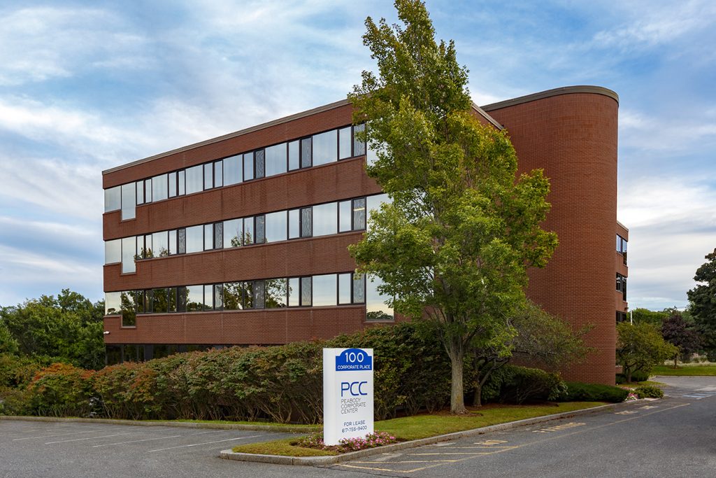
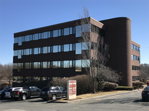
SemiNex Corporate Headquarters

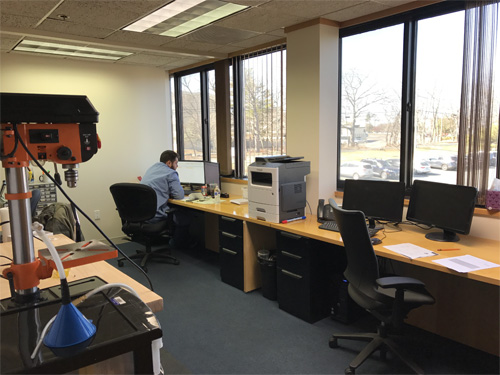
SemiNex Corporation has acquired an adjoining suite to their current headquarters in Peabody, Massachusetts effectively doubling production area and increasing office space. This move complements several rounds of hiring and paves the way for several product releases anticipated in 2019.

“For more than 10 years, SemiNex has kept costs down for customers by operating with a streamlined fabless business model,” explains David Bean, SemiNex President. “In the coming year, we’re predicting a substantial increase in demand for our wavelengths within the consumer market. Our expansion will enable us to seamlessly accommodate these new high volume orders without impacting our existing customer base.”

The new clean room facilities are designed to meet ISO Class 7 standards and ESD best practices, and are expected to be fully outfitted with upgraded test stations and equipment by January of 2019. The suite also includes office space for SemiNex engineers and process technicians.

“We’ve designed additional automation into our manufacturing processes and expanded our testing capabilities, freeing up lab space for R&D and specialty fabrication projects,” says Product Engineer Seth Pappas.

SemiNex Fuels Expansion with New Hires

SEMINEX FUELS EXPANSION WITH NEW HIRES

SemiNex Corporation announces new hires in Engineering and Marketing to support their growth in the long wavelength laser diode market. The appointments of Kenil Bhadani as Production Engineer and Stephanie Arnett as Commercial Specialist come in the advent of product innovations and expansion plans expected to launch in 2019.

A graduate of Worcester Polytechnic Institute and a Six Sigma Green Belt, Kenil Bhadani brings key experience in lean methodologies and statistical controls with his role as Production Engineer. He will manage and maintain the SemiNex production operations and drive improvements in efficiency, costs, quality, capacity and lead-times.

As Mechanical Design Engineer for Walker Magnetic, Kenil implemented a design program that specified products, Bill of Materials, overall configure price quote (CPQ) and worked according to ASME BTH-1-2014 standards to calculate tolerances of various magnets. While at Equifit in 2016, his research on the properties of Neoprene alternatives led to the successful redesign of their sports medicine boot and helped to eliminate allergic reactions.

“Kenil’s commitment to Total Quality Management principles is evident in his past work. He is well-equipped to dramatically improve our production capabilities so that customers experience better quality, performance and service,” said David Bean, SemiNex President.

Stephanie Arnett, who joins SemiNex with over 10 years of experience developing visual content and marketing strategies for brands, is responsible for raising the profile of SemiNex laser diodes as Commercial Specialist in charge of advertising and marketing efforts. Additionally, she works closely with the commercial sales team to ensure the best end to end experience for SemiNex customers.

Before working at SemiNex, Stephanie contracted with creative firms and tech companies in the Boston area on projects ranging from email marketing to virtual reality. As an early adopter of immersive photographic technology, she has produced over a hundred virtual tours and VR campaigns, including a 360º preview for a restaurant launch which generated over 100,000 views on social media.

“SemiNex is poised for a really exciting 2019. There’s a growing demand for eye-safe high power solutions as fully realized automotive LiDAR and machine vision systems are expected to be in the hands of consumers in the next few years,” Stephanie commented. “I’m thrilled to be a part of what is shaping up to be a game-changing technology.”

SemiNex Welcomes Ed McIntyre to lead Business Development

SEMINEX WELCOMES ED MCINTYRE BACK TO LEAD BUSINESS DEVELOPMENT

SemiNex Corporation is pleased to announce the return of Ed McIntyre as Business Development Manager. Ed brings more than 25 years of laser and optic business development experience to SemiNex. Over the past seven years, Ed worked for Princeton Optronics to develop business opportunities for their vertical cavity surface emitter lasers (VCSELs). He also worked at Princeton Lightwave, Inc. where he focused on the Geiger-mode 3D LiDAR cameras for defense and commercial applications.

“We’ve brought Ed back to grow our business partnerships in the consumer, medical and defense markets, but particularly in the autonomous vehicle LiDAR market,” said David Bean, SemiNex President. “With an increasing demand for eye-safe laser solutions, Ed’s experience with autonomous vehicle developers and detailed knowledge of SemiNex products will have a tremendous impact on the LiDAR market.”

“SemiNex is well positioned to support and enable autonomous vehicles,” stated Ed. “With higher optical power than VCSEL devices and longer wavelengths than the older generation LiDAR systems, SemiNex edge-emitting diodes detect objec¬ts at farther distances ensuring greater safety for passengers. Moreover, the compact design of SemiNex diodes leverages manufacturing at high volume, translating to lower costs for systems developers and consumers.”

Ed started his laser and optics sales career at Ortel Corporation in 1990, where he spent 8 years expanding their CATV and Satcom reach in the Eastern US. As Director of Worldwide Sales for Multilink Technology Corporation, he increased sales from $4 million to $135 million within three years. In 2002, Ed cultivated new applications in the defense and medical markets for volume Bragg gratings and high power lasers at PD-LD, Inc. as their Director of Marketing. In 2006, he became Director of North American Sales for QPC Lasers, Inc. and grew the business volume by 3 times in each year of his tenure. Ed joined Sheaumann Lasers as Vice President of Sales in 2008, before leading sales at SemiNex from 2010 to 2012.

“I’m excited to be back at SemiNex,” began Ed, “where I’ll be working in partnership with companies around the world to build the best laser systems imaginable.”

SemiNex Adds Principal Optoelectronics Engineer

Sidi Aboujja

SemiNex Corporation announces the appointment of Dr. Sidi Aboujja as Principal Optoelectronics Engineer to drive laser product innovations and new technologies from initial concepts into production. Dr. Aboujja is results-focused with a proven track record of developing and leading semiconductor laser technologies.

“Sidi brings 18 years of semiconductor laser experience to the table with a proven record of delivering industry-transforming new products,” announced David Bean, SemiNex President. “We are confident that his unique set of skills in laser diode chip design, wafer processing and technology development will help lead SemiNex to new markets with the most competitive products.”

Sidi is working out of SemiNex headquarters in Peabody, Massachusetts where he will develop and improve the high-power infrared SemiNex chip designs. Such development is a key factor in expanding market share in areas such as military, medical, consumer and testing, as well as other emerging markets such as automotive LIDAR and robotics. Additional responsibilities include product design, wafer processing, failure analysis, production management, yield improvement and vendor support. Sidi has experience with international product development and manufacturing.

Sidi has a PhD and MS degree in Optoelectronics & Electronics from The University of Metz in France and a second PhD in Physics from Sherbrooke University in Canada. He holds multiple scientific papers of light emission in III-V and Silicon junctions in reverse bias and was invited to present his research work in 1998 and 1999 at IEEE Nuclear and Space Radiation Effects Conference/IEEE Transaction on Nuclear Science.

At Perkinelemer Optoelectronics and Excelitas Technologies, Sidi worked as Senior Laser Scientist, Laser Project Manager and head of laser technology developments. In 2010 he completed a black belt six sigma certificate and applied six sigma tools to improve and control laser designs, wafer processing and yield improvements at Perkinelemer Optoelectronics and Excelitas Technologies. He developed many laser product lines at Perkinelemer Optoelectronics and Excelitas Technologies including single and multiple cavity laser chip and laser chip array technologies at various wavelengths and within various packages. Sidi has managed many projects from design specifications through production for a variety of markets including military, commercial, industrial and automotive, all while supporting the application engineers and product managers.

“The SemiNex laser diode is powerful and well designed,” Sidi stated. “However, there is always room for improvement. With my research and development experience I plan to apply my ideas to yield experimentally valid enhancements and major step-change improvements so that our global customer base can enjoy a wider range of capability and performance.”

SemiNex Adds Product Engineer

Seth Pappas

SemiNex Corporation announces the appointment of Seth Pappas as Product Engineer to drive product innovations in laser diode packaging and processing.

“We are excited to have Seth as our new Product Engineer,” announced David Bean, SemiNex President. “With Seth’s 20 years of experience in the photonics business, his diverse skills in product and test development will provide a fresh perspective to our company and drive innovation and value to our customers.”

Seth is working out of SemiNex headquarters in Peabody, Massachusetts as the project liaison between SemiNex and its vendors. He will manage and support various operations such as failure analysis, production, vendor support and process management, and is implementing a new test station that will provide best-in-class resolution and far-field divergence data for customers with specific ellipticity requirements. Seth will further introduce new systems to improve product marking and traceability for much of the SemiNex production line. His background in yield improvement and failure analysis will improve productivity and profitability at SemiNex.

Seth has an M.S. in Electrical Engineering and was awarded a Research Fellowship in MEMS technology. At Coretek, a small startup that developed MEMS tunable filters and tunable VCSELs for the telecom industry, Seth worked as the Test Engineer. He turned a small characterization lab into a production level test facility increasing throughput tenfold. In 2002 he joined Adaptive Optics where he produced and managed commercial wavefront sensor products and helped produce a monitoring element for the James Webb Space Telescope. From 2004 to 2006, as Senior Engineer at Boston Micromachines Corporation, Seth was responsible for manufacturing and improving BMC’s MEMS Deformable Mirror product line. He went on to Noblepeak Vision Corporation where he developed the test system for a novel germanium pixel packaged sensor array and subsequently managed the production of the TriWave SWIR camera for Infrared Laboratories. While at L3 Insight Technology, Seth helped transition a new multi-laser range-finding product from prototype to the manufacturing floor.

“I am honored to be a part of the SemiNex Corporation team,” said Seth. “This company is well-run and efficient, making its selection of products affordable and readily accessible to our many customers. I look forward to working with the SemiNex team and our vendor partners, and satisfying our customers with the best InP laser diodes.”

New Single-Mode Fiber-Coupled TO-9 Delivers up to 650mW

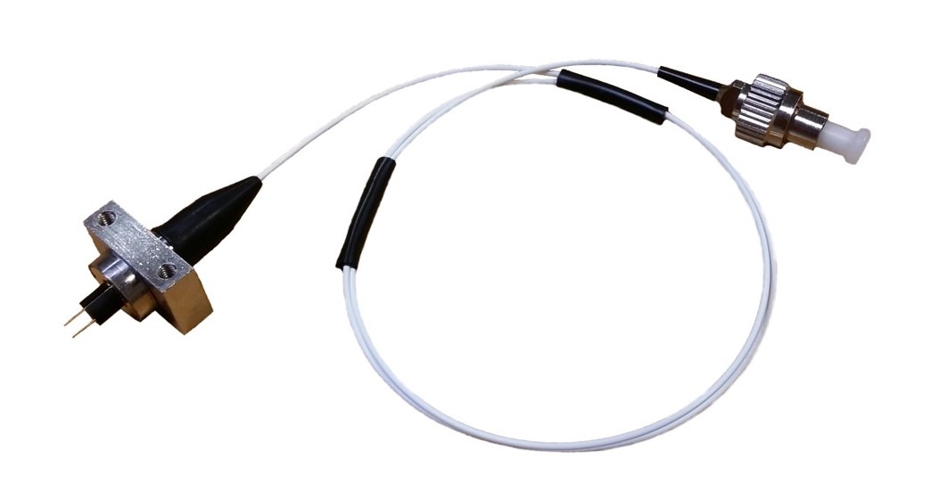
SemiNex Corporation introduces a single-mode fiber-coupled TO-9 laser diode package. This new product is ideal for customers who need fiber-coupled usability with powerful SemiNex TO-9 laser diodes.
The new SemiNex TO-9 fiber-coupled package (TO9F) delivers a simple and dependable source of infrared laser light and is the company’s latest single-mode fiber-coupled device. The TO9F is the product of choice for customers who require a small form factor fiber-coupled package for applications such as OTDR systems. David Bean, SemiNex’s President and CEO, explains, “We are pleased to expand our product line in offering the TO9F to enable customers to quickly integrate our latest high-power laser chips into their applications.”

The TO9F boasts a small form factor measuring only 17 mm wide, 10.5 mm tall and 26 mm long encased in a 17 mm x 10.5 mm x 5 mm cooling block with screw holes for effective thermal mounting. The device is coupled to a 9/125 μm single-mode fiber with a standard FC/PC connector. Patrick Dinneen, Application Engineer, states, “SemiNex is constantly aiming to improve product usability by implementing small, standardized designs leading to easier system integration. This will allow our customers to save time and money when developing a production level product.”

The TO9F debuts at the 2018 Photonics West Conference in San Francisco, CA with 1550 nm wavelength and output power of 175 mW CW at 1 A drive current. For pulsed applications (<150 ns pulse width and <0.1% duty cycle) the 1550 nm device will deliver about 550 mW of optical power. SemiNex offers the product at standard wavelengths between 1300 and 1700 nm. The 1310 nm TO9F delivers 200 mW CW and 650 mW pulsed.

Driven by high-volume manufacturing, the SemiNex TO-9 sub-mount has improved over the years as a result of many design reviews in an effort to reduce costs as well as improve materials, fabrication processes and the heatsinking design. Matthew Hamerstrom, Mechanical Engineer, goes on to say, “With our continuous improvement in both engineering and manufacturing, SemiNex is confident that it can deliver the new TO9F to our customers with effective integration, dependability and scale to volume production.”

New Medical 1270nm Wavelength debuts at 2017 World of Photonics

SemiNex Corporation debuts its new 1270nm laser wavelength at this year’s World of Photonics show in Munich. This new wavelength builds upon SemiNex’s prior range of 1300-1700nm and expands the company into new areas of the medical industry.

Vaccine

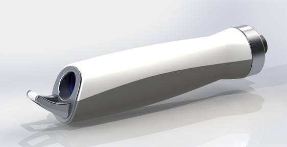
SemiNex teamed up with Veralase, LLC and Massachusetts General Hospital to develop an affordable hand-held laser device that operates at 1270nm. This specific wavelength has proven to enhance immune response to vaccines. This near-infrared laser treatment avoids side effects like soreness, inflammation, erythema and tissue damage that often occurs with chemical adjuvants. Under a U.S. National Institute of Health (NIH) grant received by Veralase, SemiNex continues to support the research of other optimal wavelengths and their potential clinical applications.

“SemiNex is proud to be a part of this groundbreaking medical research,” stated David Bean, President of SemiNex Corporation. “We are pleased to collaborate with Veralase and the amazing scientists at Massachusetts General Hospital.”

Another remarkable use for 1270nm is in creating different forms of oxygen. 1270nm irradiation in water causes photoactivation in the ground state of oxygen to create singlet oxygen. Singlet oxygen is a high energy form of oxygen which can be used in preparative organic chemistry and photodynamic therapy. The uses for singlet oxygen continue to be explored.

1270nm laser diodes set a new record at SemiNex for the highest powers and efficiencies to date. These added benefits of power and efficiency will enable customers to use small, efficient and relatively inexpensive laser diodes to develop products in many industries and applications. Dr. John Callahan, SemiNex’s Vice President of Engineering, explains, “With the new 1270nm projects, SemiNex has been able to work on optimizing high volume manufacturing processes to drive down cost and improve yields.”

Continuous improvement is a core value at SemiNex and the company plans to develop and fine-tune the new wavelength in response to customer and market needs. SemiNex is proud to be a part of improving worldwide healthcare and anticipates taking on new medical projects in the near future.

To discuss projects using the new 1270nm wavelength or any other of the company’s products, stop by and visit with us this week at Hall B3 / Booth 258 at World of Photonics in Munich or respond to the contact information below. We look forward to hearing from you!

SemiNex Doubles Manufacturing Space

SemiNex Corporation doubles manufacturing capacity and expands office and conference room spaces to better service its growing worldwide customer base. Since 2015 the number of sales leads has tripled and business volume is at record-levels. To keep pace with growing demand, SemiNex combined multiple locations into to one larger headquarters to expand operations, increase productivity and facilitate collaboration between employees. Since the move, customer response times have improved and teamwork is more robust.

Engineering

SemiNex now has a dedicated cleanroom for precision lensing of laser diodes used in medical, military and LIDAR applications. The engineering offices are nearly doubled, accommodating for additional engineering projects and staff. SolidWorks CAD and Zemax software packages were upgraded to provide state-of-the-art engineering capabilities and services. The conference space expanded allowing for twice the occupancy and is equipped with the latest videoconference and computer systems. Shipping and receiving is now located conveniently next to inventory and testing clean rooms. The flow of information and outgoing products is more streamlined allowing for increased shipping and handling speeds.

“We look forward to serving our customers even more effectively, while enjoying a more comfortable and productive office space as employees of SemiNex,” stated David Bean, SemiNex President.

Peabody, MA

The new SemiNex Corporation address is:

SemiNex Corporation
100 Corporate Place

Suite 302
Peabody, MA  01960
USA
+1 978-326-7700

SemiNex remains in the same building as before with consolidated operations on the 3rd floor in Suite 302.

Be sure to visit if you are in the area!

New 4CM: High Power and Small Form Factor

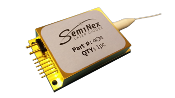
SemiNex Corporation now offers the 4CM, a multi-chip fiber-coupled laser module with up to 14 Watts of CW power in a single core fiber. After great success with the 2CM introduced just a couple years ago, SemiNex Corporation now offers nearly double the power with the same high standard of quality and reliability.

Like the 2CM, the 4CM optically combines the beams of multiple internal laser chips into a single core fiber offering high power and high conversion efficiency. SemiNex’s MCM (Multi Chip Module) also offers high power and high brightness, but coupled into a bundled fiber pigtail. While this design offers options for fusion splicing and laser bar coupling, energy is lost due to coupling efficiency. The 4CM delivers a simpler design in a smaller and more reliable package.

The 4CM is now offered at 1310, 1470 and 1550 nm, all of which are known eye-safe wavelengths making it highly desirable for medical applications. The product features a single 0.22 NA 400µm fiber with an SMA 905 connector. An aiming beam, photodiode, and thermistor all come integrated into the module.

“The 4CM is the next generation laser module in the SemiNex product line,” explained Dr. John Callahan, SemiNex’s Vice President of Engineering. “This product offers higher power in a single core fiber and can be configured across our entire wavelength range of 1300 to 1700 nm.”

Applications like surgical treatments, laser radar, and industrial measurement will greatly benefit from this new product. The 4CM is expected to enable new and improved deployments of laser diodes into various applications. SemiNex engineers are available to assist customers in designing the best laser diode for their application.

SemiNex Joins Forces with Dolleris and Enhances the Medical Industry

SemiNex Corporation, a leading supplier of high-power InP lasers between 1300 and 1700nm, and Dolleris Scientific Corporation, a company that designs and manufactures a variety of products, have entered into a multi-year exclusive contract to produce a high-power laser system for professional medical applications.

The SemiNex Engineering Team spent the better part of the past three years working with Dolleris Scientific to design a custom laser and lens assembly that achieves the required performance. Because of the flexibility of the ultimate design specification, rapid prototypes were produced and SemiNex was able to move into production within 2 months.

David Bean, SemiNex’s President stated, “Working with the Dolleris team is a pleasure. They clearly defined requirements and we were able to apply our leading-edge technology to design a robust solution that met their requirements in terms of power, performance, form factor, cost and warranty.”

Dolleris Scientific is integrating SemiNex 1470nm wavelength lasers into an existing baseline system for dermatological treatments. The private-label customer has a base unit for treating a wide variety of medical and cosmetic conditions in more than 50 countries worldwide. The SemiNex laser will compliment this suite by adding new treatment options. “It is a pleasure to collaborate with SemiNex … from developing new applications and beyond, into multi-year production planning of new products,” remarked J. Enemaerke, President of Dolleris Scientific. “SemiNex’s willingness to work with small companies in the early stages of product development, and continued support as delivery schedule demands change during production shows dedication to a mutually beneficial long-term business relationship.”

Mr. Bean added, “SemiNex looks forward to continued collaborations with the Dolleris Scientific team. By working together, we are able to expand our product lines and technologies.”

en_USEnglish